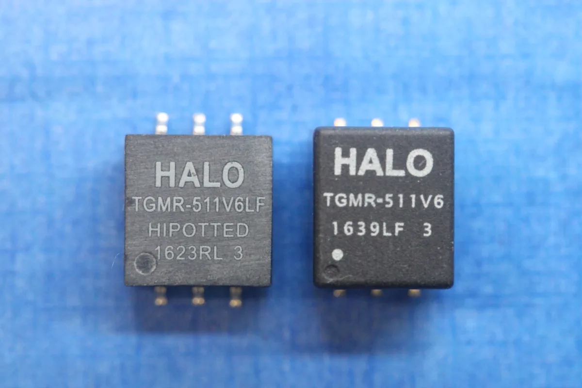
Welcome to another exploration of the fascinating world of electronics. Today, we dive into the heart of every modern device — the microchip.
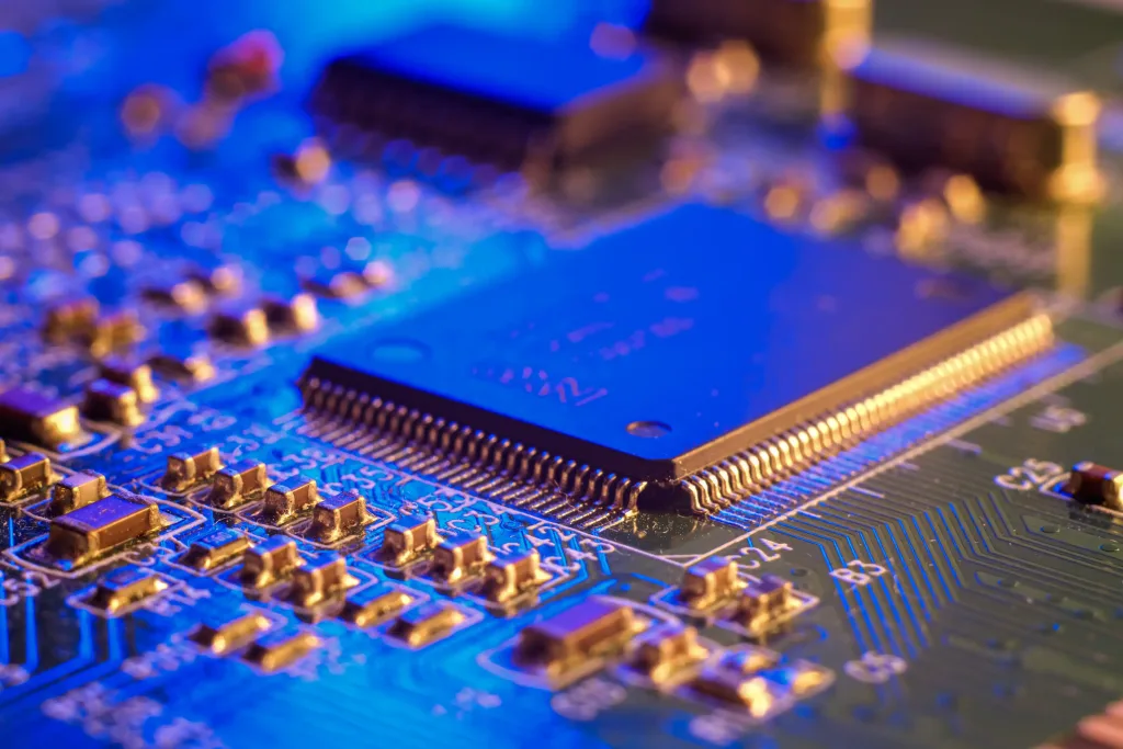
Also known as an integrated circuit (IC), this tiny component plays an essential role in the functioning of everything from smartphones to satellites.
Let’s break down what makes microchips so vital and complex.
What is a Microchip?
The Basics
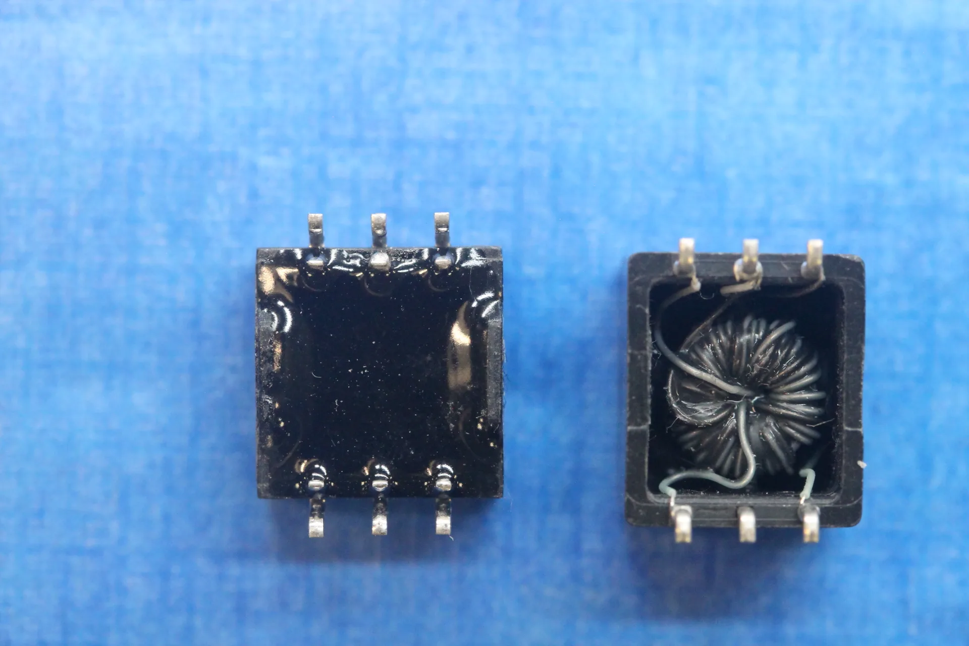
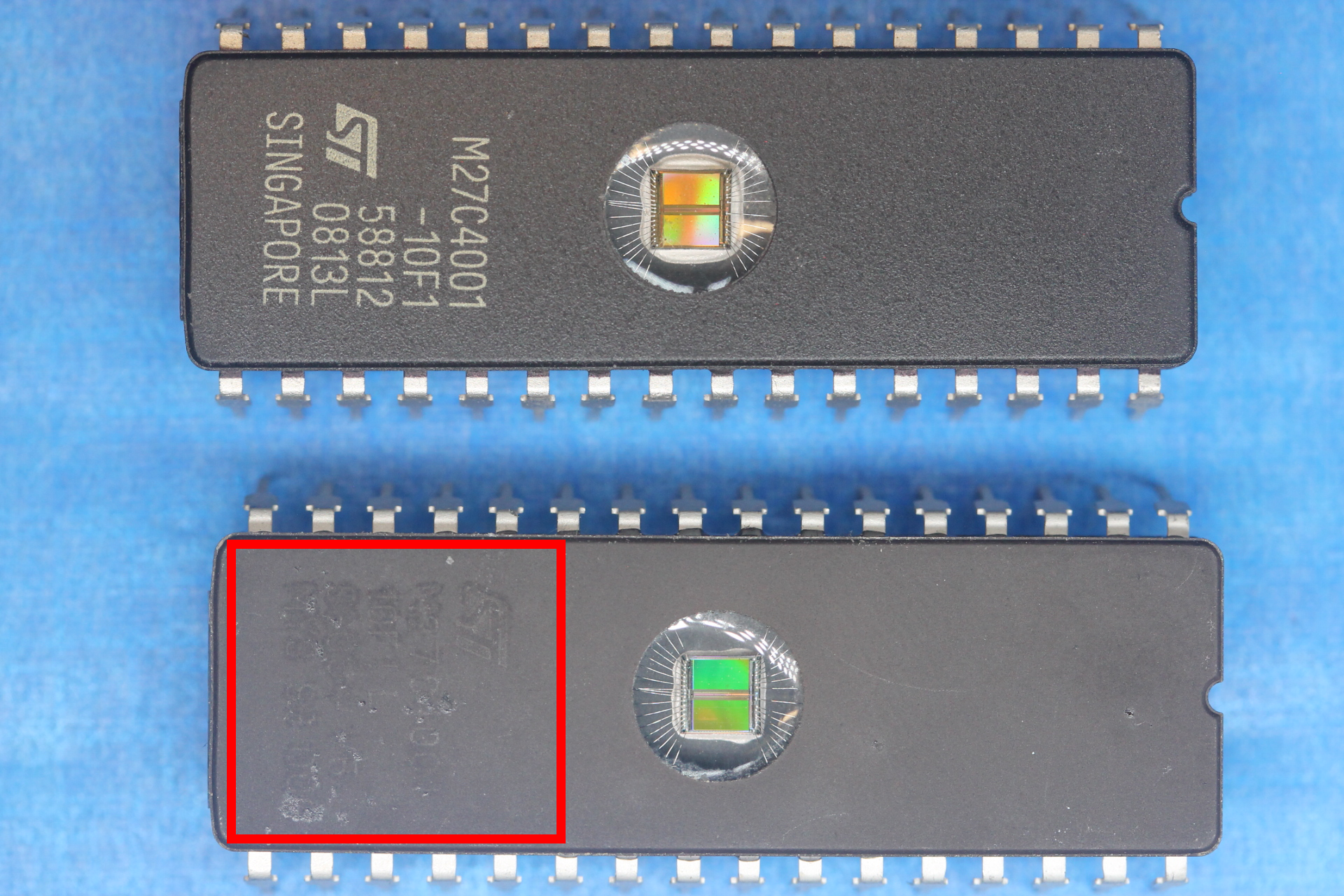
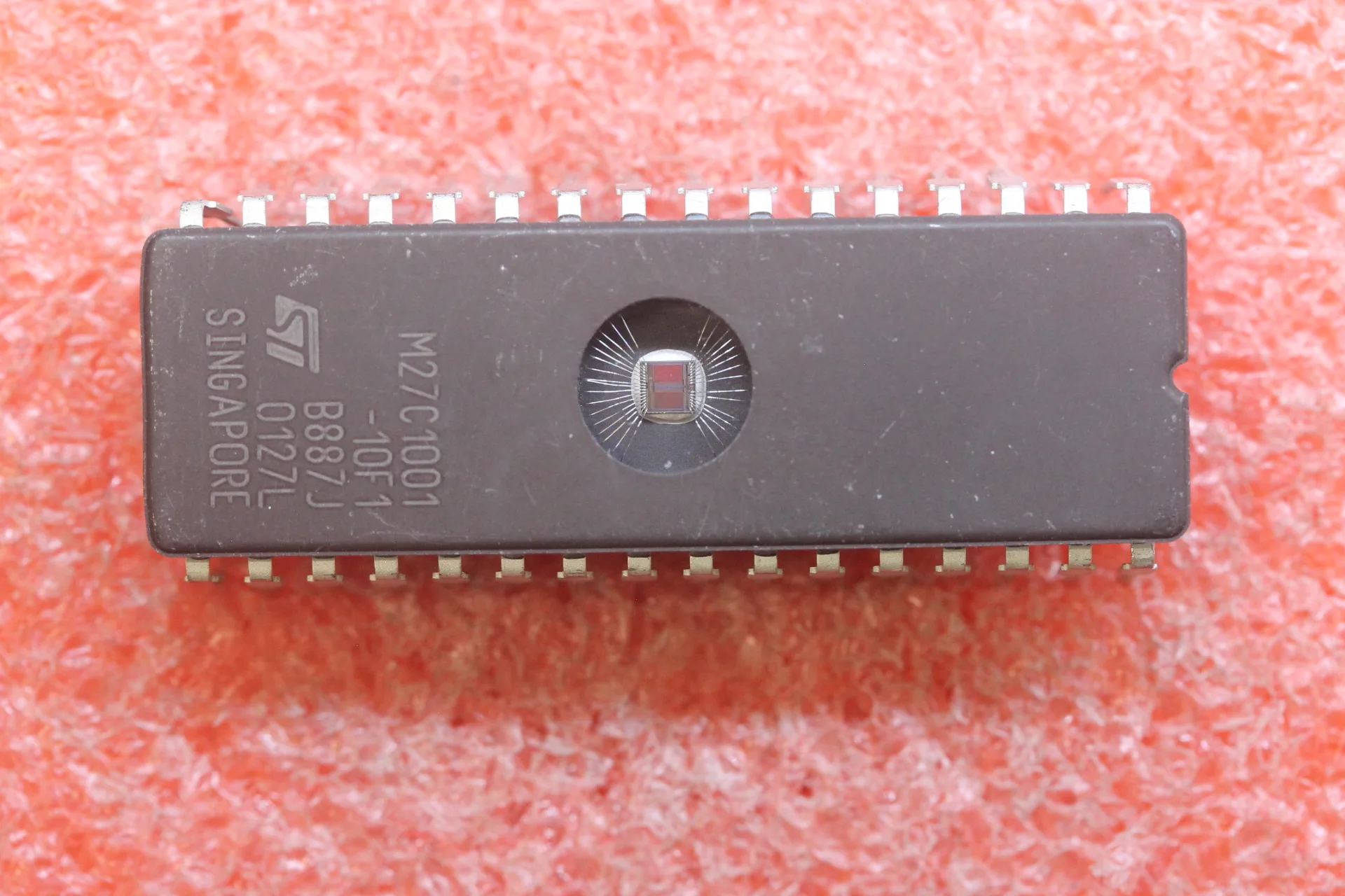
A microchip, or integrated circuit, is a set of electronic circuits on a small flat wafer of semiconductor material (usually silicon) called a “chip.” This compact unit forms the core of all digital devices, performing operations through electrical signals.
Silicon: The Star Player
At the base of most microchips is silicon, derived from silica sand. This sand is processed, melted, and recast into ingots which are then sliced into thin wafers to serve as the foundation for microchips.
The choice of silicon is due to its semiconductor properties, which can be changed or enhanced by adding materials like boron or phosphorus, allowing for precise control over electrical currents.
The Evolution of Microchip Technology
Shrinking Sizes
Microchips have been on a remarkable journey of miniaturisation. Currently measured in nanometres (a millionth of a millimetre), the features of chips are now so small they are soon expected to be measured in angstroms — a unit of measurement used for atoms and wavelengths of light. This continuous reduction in size allows more components to fit onto a single chip, enabling them to perform increasingly complex functions.
The Cost of Complexity
As microchips have evolved, so too has the technology required to manufacture them. Advanced and costly equipment is now necessary to produce the minute features of modern chips, reflecting a significant investment in pursuit of higher performance and efficiency.
Types of Microchips
Microchips can be categorised based on the type of signal they handle:
- Digital chips process binary signals (ones and zeroes) and include processors and memory chips.
- Analog chips use continuous signals, performing tasks in devices that require a range of values, like sound equipment.
- Mixed-signal chips combine both digital and analog functionalities, useful in complex applications like communication devices.
Specialised Chips: ASICs and SoCs
ASICs (Application-Specific Integrated Circuits) are designed for specific tasks, such as processing digital signals in mobile phones.
SoCs (System on a Chip) integrate multiple chip functions onto a single microchip, which is crucial for the efficiency and performance of small, portable devices like smartwatches.
The Future of Microchips and Moore's Law
Proposed by Gordon Moore in 1965, Moore’s Law theorises that the number of transistors on a microchip will double approximately every two years.
This prediction has held true for decades, mirroring continued growth in computational power and miniaturisation. However, we are now approaching physical limits where transistors are nearing the size of atoms, suggesting we may soon see an end to this trend.
Microchips and the Tech Boom
This miniaturisation and power boost from microchips has enabled groundbreaking advancements like virtual reality, on-device artificial intelligence (AI), and high-speed data transfer through 5G networks. Microchip technology is also the foundation for complex algorithms used in deep learning, a cornerstone of AI development.
How Cyclops Electronics Can Help
At Cyclops Electronics, we specialise in sourcing hard-to-find electronic components and the reliable supply everyday parts that keep your operations running smoothly. Whether you are tackling a challenging project or looking to maintain steady production with high quality components, our team of dedicated experts is here to assist you.
Discover how we can help you navigate the complexities of electronic sourcing and ensure you have the parts you need when you need them.
We are your partners in procurement, ready to support your projects with our expertise and vast network.